Showing posts with label BLOG. Show all posts

Thursday, 10 October 2019

N-type and P-type semiconductor

In semiconductor physics Group IV( in IUPAC Notation it is Group 14) contains Carbon (C), Silicon (Si), Germanium (Ge), Tin (sn), Lead (pb), Flerovium (Fl), all this elements contains 4 electrons in its outer shell nothing but four valence electrons. Out of all this elements Silicon (Si) is widely used in fabrications of chips because of following advantages.

  • Silicon reacts with oxygen and forms oxides itin a controlled manner and forming a layer of stable oxide which reduces thesurface recombination velocity
  • Its hardness that allows large wafer to behandled safely
  • Its thermal stability, up to 1100o C,that allows high temperature processing related to diffusion, oxidation andannealing
  • Primarily available for low cost

By adding an impurity conductivity of material can be increased and depending on the impurity added we can have two types of semi-conductors
N-type Semiconductor :
When the group V element is added to the intrinsic or pure semiconductor (silicon or Germanium), the resulted product is said to be an n-type semiconductors. The group V elements are phosphorus, arsenic, antimony and this elements have five valence electrons. When Phosphorus is added to silicon, it forms four covalent bonds with neighbouring silicon atoms. The fifth valence electron of phosphorus atom does not involve in formation of covalent bond and this electron is free to move in structure. As the group V elements donates a free electron, these elements are called donors. With small addition of impurity (phosphorous) provides millions of electrons which are majority carrier in n-type semiconductor

                                             N-Type Semiconductor

P-type Semiconductor
When the trivalent impurity or acceptor impurity added to Silicon (Group IV), the resulted product is said to be p-type semiconductors. The group III elements are Boron (B), Gallium (G), Indium (In), Aluminium (Al) and these elements has three valence electrons. When Boron in added to Silicon as impurity, three covalent bonds are formed with three neighbouring silicon atoms and in fourth covalent bond, only silicon atom contributes one valence electron, while the boron atom  is in short of one valence electron. Thus the fourth covalent bond is incomplete with shortage of electron and this missing electron is called hole. With small addition of impurity (boron) provides millions of holes which are majority carriers in p-type semiconductor

                                                       P-Type Semiconductor

Wednesday, 9 October 2019

VIM editor series II

Here is second post on the vi editor commands.
Insert a file content

:r file_name or file_path

example: Need to paste the info from file B to A      

           Copied the content to file A from file B using command :r B 

Repeat the Last Action 

. (dot or aka period or full stop)

  • Suppose you press dd to delete the line. Next if  you want to delete the next line you press dd or .(dot)
  • Suppose you press Hi and you like to repeat the action then just press .(dot) in normal mode of vi editor

Display the line numbers
enable the line number 

:set number or :set nu 

disable the line numbers

:set nonumber or :set nonu

Reversing the Order of lines 

:g/^/m0

:—- start the command line mode

g—- action will be taken all lines in the files
^—-matches the starting of the line
m—moves the elements
0—Is the destination line, beginning of the buffer

If i need to reverse the lines between a certain range(like between 30 and 40 lines), then we can use the following command
:30,40g/^/m29

To control the position of split window
:set splitbelow or splitright

Undo and Redo
In normal mode conditions

  • use u for undo the action
  • cntrl+r for redo the action 

Tuesday, 8 October 2019

Conductors,Insulators, Semiconductors

At present we can find chips in every application, even in space application. And silicon (Si) is widely used material for manufacturing the chips. Semiconductors materials are used mostly in chips. Based on Energy Band gaps the metals are classified into

  • Conductors
  • Insulators
  • Semiconductors

A band gap is the distance between the valence band of electrons and the conduction band of electrons. A band gap is minimum energy required to excite an electron to conduction band from a valence band

Conduction band is the band of orbitals that are high in energy and are generally empty at room temperature. In reference to conductivity, it is the band which accepts the electrons

Valence Band is the band occupied with molecular orbitals which are lower in energy. When there is temperature raise, the electron will jump from the valence band to conduction band, making the materials conductive

Fermi Level is defined as highest occupied molecular orbital in valence band at 0 k. The Fermi level lies between the valence band and conduction band because electrons will eventually occupy the low energy states at room temperature. Fermi level can be considered as sea of electrons above which no electrons will exits. Fermi level changes as the solids are warmed and electrons are removed or added to orbitals

Conductors
In conductors the valence band and conduction bands are overlapped. This overlap causes the valence electrons to move freely in conduction band which results in conduction. Metals, living beings are few good conductor materials. This materials offers less resistance to flow of electrons.

                                            Fig 1 : Conductors

There is no band gap in conductors and electrons are free to move to conduction band.

Insulators
In Insulators the conduction band and valence band are separated with large band gap. This prevents the electrons movement between the valence band and conduction band. And there will be no conductivity. Wood, plastic, glass are few of the insulating materials. This material offer more resistance to flow of electrons.

                                         Fig 2: Insulators

Semiconductor
In the semiconductors the band gap energy is small, as a result with small amount of heat or energy electrons get excited and jumps from the valence band to conduction band. There will be conduction of electricity and with small amount of doping conductivity of materials will be increased. In this material we can control the flow of electrons.

                                        Fig 3: Semiconductors

There are two types of semiconductors.

  • N-type Semiconductor electrons are majoritycarrier for electricity and hole are minority carriers
  • P-type Semiconductor holes are majoritycarrier for electricity and electrons are minority carriers

Monday, 7 October 2019

Verilog code for PWM Generator

Pulse Width Generator Model
PWM.v

module pwm(clk_in,sw0,rst,sine_ampl,div_factor_freqhigh,div_factor_freqlow,pwm_out);

parameter width_p = 10'd12;                                             

input clk_in;

input rst;                                                          

input sw0;

input [width_p-1:0] sine_ampl;                                        

input [31:0] div_factor_freqhigh;                                     

input [31:0] div_factor_freqlow;                                      

output reg pwm_out;                                                    

parameter load_new_ampl = 3'd0;

parameter pwm_high = 3'd1;

parameter pwm_low = 3'd2;

wire ce_w;                                                          

reg [2:0]state_r;                                                     

reg [2:0]n_state;                                                                    

reg [12:0]treshold_r =20'd0;

reg [12:0]count_r = 20'd0;

frequency_trigger freq_ce (clk_in, sw0, div_factor_freqhigh, div_factor_freqlow, ce_w);

always @ (posedge clk_in or posedge rst)

 begin

  if(rst)

  state_r<=load_new_ampl;

  else

  state_r  0)

   n_state <= pwm_high;

   else if (sine_ampl == 0)

   n_state <= pwm_low;

 end

pwm_high:

 begin

  count_r = count_r + 1;                                        

   if ((count_r <((2**width_p)-1)) && (count_r < treshold_r))

    n_state <= pwm_high;

   else if (count_r == (2**width_p)-1)

    n_state <= load_new_ampl;

   else if (count_r < ((2**width_p)-1) && (count_r == treshold_r))

   n_state <= pwm_low;

 end

 pwm_low:

  begin

  count_r = count_r +1;                                           

  if (count_r < ((2**width_p)-1))

  n_state <= pwm_low;

  else if (count_r == ((2**width_p)-1))

  n_state <= load_new_ampl;

 end

endcase

end


always @(posedge clk_in)

begin

 case (state_r)

 load_new_ampl: pwm_out = 0;

 pwm_high: pwm_out = 1;

 pwm_low: pwm_out = 0;

 endcase

end

endmodule

===================================

frequency_trigger.v

frequency_trigger(clk_in,sw0,div_factor_freqhigh,div_factor_freqlow,freq_trig);

input clk_in;                       

input sw0;                       

input [31:0] div_factor_freqhigh;

input [31:0] div_factor_freqlow;

output reg freq_trig;            

 integer freq_cnt=12'd0;          

 always @(posedge clk_in)

  begin

   freq_trig = 1'b0;             

   freq_cnt = freq_cnt + 1;    

  if (sw0 == 0)

   begin

   if (freq_cnt >= div_factor_freqlow -1)

    begin

    freq_trig = 1'b1;

    freq_cnt = 'd0; //reset

   end

  end

  else

  begin

  if (freq_cnt >= div_factor_freqhigh - 1)

  begin

  freq_trig = 1'b1;

  freq_cnt = 'd0; //reset

  end

 end

end

endmodule

==============================

Finally we need test bench to run the simultions and check the functionality of the design

pwm_testbench.v

module pwm1_tb();

parameter cntampl_value_p = 8'hff;           

parameter depth_p = 8'd8;                      

parameter width_p = 10'd12;                  

reg clk_in_r;

reg rst_r;                                   

reg sw0_r;                                     

reg [(width_p-1):0] sine_out_w;                    

wire pwm_out_w;                                  

  pwm dut2 (clk_in_r, sw0_r,rst_r,sine_out_w, 1, 2, pwm_out_w);

initial

begin

rst_r=1'b1;

clk_in_r = 1'b1;

 end

 always #10 clk_in_r = ~clk_in_r;

initial

begin

#50000 rst_r=1'b0;

 sw0_r = 1'b0;

 sine_out_w=3000;

 #163860  sine_out_w=4220;

 #163860 sine_out_w=2376;

 #163860 sine_out_w=5856;

 #163860 sine_out_w=1237;

 #163860 sine_out_w=5856;

 #163860 sine_out_w=5984;

 #163860 sine_out_w=5598;

 #163860 sine_out_w=4763;

 #163860 sine_out_w=3624;

 #163860 sine_out_w=2376;

 #163860 sine_out_w=1237;

 #163860 sine_out_w=402;

 #163860  sine_out_w=16;

 #163860 sine_out_w=147;

 #163860 sine_out_w=771;

 #163860 sine_out_w=1780;

 #163860 sine_out_w=3000;

 end

initial

#200000000 $finish;

endmodule

================================

Digitally Controlled PWM Generator

Design specification
Design and implementation of  architecture of Frequency trigger, Finite State Machine (FSM) for generating the PWM signal ,Pulse Width Modulation.
Input   :  clk,
Input   : [11:0]sin amp
Input   : switch0,fmhigh,fmlow.
Output: [1:0] pwm

Depending upon frequency high(fmhigh), frequency low(fmlow),frequency trigger will generate different  waveforms. By using fsm we design  Pwm model. 

Architecture for the design specification 

                                                             Fig 1: FSM
                                                       Fig 2: Block diagram

 Manual calculation
PWM is modulation technique used to encode a message into a pulsing signal. In PWM Ton denotes the one time and Toff denotes the off time of signal. Period is the sum of both on and off times and is calculated as shown below.

  Ttotal =Ton +Toff

Duty cycle is calculated as on time to the period and duty is calculated as below

D=Ton /(Ton + Toff)
 D= Ton/Ttotal

PWM Signal when used at a different duty cycles gives a varying voltage at the output. This method is used in various applications like:

  • Switching regulators
  • Led dimmers
  • Audio
  • Analog signal generation
  • Speed control of Motors

The out voltage is calculated by following equations

Vout  = D*Vin
Vout =(Ton /Ttotal)*Vin

  verilog code in next post      

Sunday, 6 October 2019

VIM editor series I

Search A Pattern

  • Press Esc
  • Then type / or ? and the pattern need to search

To do Substitution

:%s/Old String/New String/g 

Converting the Tab to Spaces

:set expandtab 


To control the number of space character need to be inserted when the tab was used

:set tabstop=4 

After the expandtab option is set all the new tab characters entered will be changed to spaces. This will not affect the exiting tab characters. To change all the existing tab characters to match the current tab settings use

:retab 

Display the line numbers
enable the line number

:set number or :set nu 

disable the line numbers

:set nonumber or :set nonu 

Reversing the Order of lines

:g/^/m0


:—- start the command line mode
g—- action will be taken all lines in the files
^—-matches the starting of the line
m—moves the elements
0—Is the destination line, beginning of the buffer

If i need to reverse the lines between a certain range(like between 30 and 40 lines), then we can use the following command

:30,40g/^/m29 

To control the position of split window

:set splitbelow or splitright 

Undo and Redo
        In normal mode conditions

  • use u for undo the action
  • cntrl+r for redo the action        

Saturday, 5 October 2019

Perl_Series II

Hashes
A hash is an un-ordered group of KEY-VALUE pairs and keys are unique strings(duplication of keys are not allowed). The values are scalar and they can be either a number ,a string or a reference. These are also called as associative arrays.

Before using the hash we have to first declare it 

my %hash ;

As I said above duplication of keys are not allowed and this property can be used to list out the elements without any repetition. Let us consider a array of numbers with repetition.
@numbers =(0,2,3,4,1,4,2,2,3,5,5)

my @unique;
my %hashes;
my @numbers =(0,2,3,4,1,4,2,2,3,5,5);
foreach my $value (@numbers) {
  if (! $hashes{$value}) {    
push @unique, $value;   $hashes{$value} = 1; 
}}
print @unique;

output:023415

Tuesday, 1 October 2019

Cell Delay of Standard Cell and what are the factors effecting the cell delay

Cell Delay:
Time between a 50% transition on input to 50% transition of output waveform. It is also called as

  • Gate delay
  • Propagation delay
                                                      Cell Delay

The gate/cell delay is not constant for all design environmental conditions. Cell delays are calculated using Non Linear Delay Model(NLDM) and the cell/gate delay depends on the input transition and output load

cell delay ={input transition time,Output load}

Input Transition Time :
Time taken by signal to reach 20% to 80% of peak value(rise signal)  or to reach 80% to 20% of peak value(falling signal)

                                       Transition time (rise & fall)

Output Load:
Output load is total capacitance value that is connected to output pin of the cell

 Cload =Cnet+Cpin

Cpin —————-Input capacitance of the driving pin
Cnet —————–Intterconnect capcitance
All this values(input transition time and output load) are provided in lib(timing libray) files of the standard cells and below is snippet of .lib files.


***********snippet of lib file of as standard cell*********************
pin(“PhyInitSync[1]”) {
related_power_pin : VDD;
related_ground_pin : VSS;
direction : input ;
max_transition : 0.150000 ;
capacitance : 0.001672 ;
/* Other user defined attributes. */
original_pin : PhyInitSync[1];
 timing () {
  related_pin : “DfiClk” ;
timing_type : setup_rising ;
rise_constraint( f_dtrans_ctrans ){
index_1 ( “
0.001000, 0.010000, 0.020000, 0.040000, 0.080000, 0.120000, 0.150000″);
index_2 ( “
0.000000, 0.002388, 0.004669, 0.010000, 0.017848, 0.034895, 0.090000″);
values ( “
-0.001922, -0.002219, -0.002587, -0.003267, -0.003591, -0.003837, -0.003263″,\
“0.000255, -4.09999999999994e-05, -0.000410000000000001, -0.00109, -0.001414, -0.001659, -0.001086”,\
“0.001887, 0.00159, 0.001222, 0.000542000000000001, 0.000217, -2.80000000000002e-05, 0.000546”,\
“0.003733, 0.003436, 0.003068, 0.002387, 0.002063, 0.001818, 0.002392″,\
“0.005476, 0.00518, 0.004811, 0.004131, 0.003807, 0.003562, 0.004135”,\
“0.006344, 0.006047, 0.005679, 0.004998, 0.004674, 0.004429, 0.005003”,\
“0.00663, 0.006333, 0.005965, 0.005284, 0.00496, 0.004715, 0.005289”);
}
fall_constraint( f_dtrans_ctrans ){
index_1 ( “
0.001000, 0.010000, 0.020000, 0.040000, 0.080000, 0.120000, 0.150000″);
 index_2 ( “
0.000000, 0.002388, 0.004669, 0.010000, 0.017848, 0.034895, 0.090000″);
values ( “
0.0075, 0.007203, 0.006834, 0.006154, 0.00583, 0.005585, 0.006158″,\
“0.010092, 0.009795, 0.009427, 0.008747, 0.008422, 0.008177, 0.008751”,\
0.012482, 0.012185, 0.011816, 0.011136, 0.010812, 0.010567, 0.01114″,\
0.012482, 0.012185, 0.011816, 0.011136, 0.010812, 0.010567, 0.01114″,\
 “0.015991, 0.015694, 0.015325, 0.014645, 0.014321, 0.014076, 0.014649”,\
………………….
………………….
………………….
}}

For corresponding output load and input transition we can get the cell delay values from the tables provided in the .lib files. Index 1 represents the input transition ,Index 2 represents the output load and the values represents the delay of the cell. Lets us see how does the tool picks the delay value from the NLDM table

Assume the input transition as 0.02 and the output load as 0.01 for particular environment/corner and the value marked red in the values table gives the cell delay(0.003068) for the given input transition and output load. Have u guys noticed above rise_constraint and fall_constraint table, we can calculate the cell delay from both the tables.Then which cell delay value does the tool pick for the analysis  ?

For the setup analysis mode the tool picks which ever cell_delay value is max .
For the Hold analysis mode the tool picks which ever cell_delay value is min .


Up or Down counter which is better

Up Counter:
The counter which counts from 0 to finite value
Down Counter:
The counter which counts from finite value to 0

For a Design if both up and down counter works equally well, then which one should be selected?
Up counter will be the best option compared to the Down counter because we need a two’s complement circuit in down counter which takes extra logic. This increases the no of gates and power consumption.

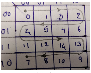
In grey counter only one bit is toggled at each time and this counter is used in pointing the memory locations and simple way to remember the grey count seqeunce


4-bit grey Counter
0000 – 0                                1101 – 12
0001 – 1                                1111 – 14
0011 – 3                                1110 – 13
0010 – 2                                1010 – 9
0110 – 6                                1011 – 10
0111 – 7                                1001 – 8
0101 – 5                                1000 – 7
0100 – 4
1100 – 11


Monday, 30 September 2019

how to design the better transistor which has high on current and low off current

Speed of the transistor is decided with Ion and Ioff. On current was increased as we go down the technology node because less Vt is required for small channel length and delay of the device is also  reduced.When Device is off(i.e Vgs =0 and Vds=Vdd) there will be subthreshold current which contributes to the Ioff current and this current must be maintained low to reduce the static power. For better operation of the devices on current must be high and off current must be low.

  • Ion current was increased with decrease in Vt ( this is reduced for every latest technology node)
  • Ioff must be maintained low and this is achieved by reducing the subthreshold swing. Vt can be increased to reduce the Ioff but this will affect the Ion current of the device and delays of the devices will be affected.

Below image gives the equations of Ioff current and sub threshold swing 
W  represents the width of the channel
 L    represents the length of the channel
Vgs  represents the gate to source voltage
Cox  represents the oxide capacitance
 Vt represents the threshold voltage of the devices.


 From the above equations we can say Ioff can be reduced by changing S(subthershold swing) ,this can be achieved two ways

  • By Increasing the Cox i.e. using thinner oxide 
  • By reducing Cdep of the device, this can be done by increasing Wdep.
                                              nmos(source:internet)

Oxide capacitance can be increased by using the thinner oxide or high dielectric materials. Thickness of the oxide layers cannot be reduced beyond the 1nm , if it is beyond the 1nm , there will be a breakdown of the oxide material and tunnelling leakage current increases.
Because of the above limitation in thickness researchers started using the high K dielectric materials. Like 6nm thick HFO2 is equivalent to 1nm thick of Sio2 in the sense that both the films produce the same Cox. Like very solution as some negative effect, high K dielectrics are highly unstable and they react with the substrate.By inserting a thin Sio2 layer  between substrate and dielectric material the chemical reaction can be reduced. High K dielectric materials offer lower surface mobility than Si/Sio2 which is a disadvantage . 
Cdep can be reduced by increasing the Wdep, this can be done by decreasing the doping concentration because Wdep is inversely proportional to Nsub (doping concentration).
For a Device to work properly, we need to change Wdep, Tox, Xj(drain junction depth) proportional  to change in channel length 


Thursday, 26 September 2019

Temperature effects on Mobility

In a Cmos or Finfet the current flow is due to movement of the electrons and holes. The free movement depends on the mobility of electrons/holes and factors affects the mobility are lattice scattering and impurity scattering which are dependent on the temperature.

Lattice scattering
Atoms vibrate more as the temperature increase and this results in collisions with another atoms and causing carriers (electrons/holes) to be free. This collective vibration is called phonon, thus it is also called as phonon scattering. Therefore with increase in temperature the vibrations of atoms increases and more carries are scattered from atoms, this increases the collision between the electrons and reduces the mobility. Despite the decrease in mobility, conductivity increase with the temperature as carrier concentration increases with temperature. Mathematical relation between the mobility and temperature as follows


 Impurity scattering
Impurity scattering is observed in the doped semiconductors. At room temperature the impurities are ionized, and there is electrostatic attraction between the electrons travelling in the lattice and the impurities. As temperature increases the mobility of electron increased which is quite opposite to the Lattice scattering. Impurity scattering is more dominate only at low temperature in doped semiconductors. For better understanding, the electron can travel faster with increase in the temperature and it can escape the attraction forces of the impurity ions. Mathematical relation between the mobility and temperature as follows


we can observe only lattice scattering in intrinsic semiconductor where as in doped conductors we can see lattice and impurity scattering which effects the mobility of the electrons/holes.

In less doped semiconductors, the lattice scattering dominates and thus mobility decrease with increase in temperature.

For heavily doped semiconductors at low temperature as temperature increases the mobility of electrons increases since impurity scattering dominates and at high temperature the mobility decrease since lattice scattering dominates

                                           source: Image from google

False Paths:set_false_path

During the timing analysis, tools verifies whether logic paths meets all the constraints defined in the SDC (Synopsys design constraints) and reports violation if any logic paths doesn’t meet the required timings. And the tools are not intelligent enough to find which logic path was true or false path. Therefore, we must inform the tool which are the false paths before performing the timing analysis. Few cases are mentioned below.
Case I


During the Functional mode the select line of mux is tied to 0 and tool should not perform the timing analysis on this path (marked in orange) which will be active during DFT test mode. This information must be provided to the following command
set_flase_path -to <list of end points>


Case II:
We need to add false path on the pins which are tied to low or high (static signals). As they are static signals, timing checks are not necessary.
set_false_path -from [get_ports A]

Case III:
If two clocks are not related to each other (Asynchronous) then we must define these paths as false path. In this case to avoid any setup/hold violations at capturing registers some synchronizers technique must be employed. Few of the techniques are

  • Two flop Synchronizers
  •  FIFO
  •  Handshaking protocol

set_false_path -from CLKA   -to CLKB


In case of the two flip flop synchronizers as show in above figure timing checks are not necessary between the Launching flop and the 1st stage of the synchronizers. Therefore, we have to consider the signal to Flop FF2 as false path

Sunday, 22 September 2019

Technology/Process node

If you look back in time every semiconductor companies started to scale their device by reducing the area to half of its previous version.Reduction in size of devices reduces the effective capacitance, which in  turn reduces the delay (by 30 %) and makes the devices run faster. As a result Operating frequency increases.Finally to keep the electric field, the voltage for the new node need to be reduced by 30 % and this way for each technology node upgrade transistor density doubles with same power consumption


To double the density of the devices ,the contacted Poly pitch(CPP) and minimum metal pitch (MMP) need to be scaled down by roughly 0.7x each node. In other words, scaling of (7*CPP)*(.7MMP)=area/2. In this way future technology node was decided
180nm*.7 ≈ 130nm
130nm*.7 ≈  90nm
90nm  *.7 ≈  65nm
65nm  *.7 ≈  45nm
45nm  *.7 ≈  32nm
32nm  *.7 ≈  22nm
22nm  *.7 ≈  15nm
15nm  *.7 ≈  10nm
10nm  *.7 ≈   7nm
7nm*.7 ≈ 4.9nm

Before 32nm, the process node roughly corresponds to the minimum value of drawn gate length and the channel length used to be lower than the node value considering overlap from source and drain regions on gate area. Digital circuits that are synthesized using standard cells and the height ,width of standard cells are multiple of CPP and MMP as shown below

For 32nm process, different foundries had the value of these pitch around 110-130nm. if a foundry can fit a complete MOSFET device i.e source , channel and drain in one gate pitch, the absolute value of gate length would not matter and the area of the digital IC will scale with the product of metal pitch and metal pitch. So to reduce the area further, it makes sense to reduce the pitches. By scaling metal and gate pitchs, foundries continue to offer process improvements without reducing effective channel length. And with this approach ,the correlation of gate length and the node name became dilute.In the 2009 ITRS, the references to the term ‘technology node’ were eliminated. Also, roughly after this time, the process nodes scaled in a way that could be described as equivalent scaling in which the 3 dimensional device structure was improves or scaled to improve performance. As far as the names of latest process nodes such as 14/10/7 are concerned they are simply a commercial name for a generation process technology, with no relation to gate length, metal pitch or gate pitch.

Now if i say 28nm technology , we have 28nm, 30nm, 35nm, 40nm different gate length options. And the technology node will take the minimum gate length.Every thing  looks good till here but why we need different gate length for a technology node because in some design the minimum timing is met with 30nm gate length and in some other design minimum power is achieved with different gate length.  For 32nm process, different foundries had the value of these pitch around 110-130nm. if a foundry can fit a complete MOSFET device i.e source , channel and drain in one gate pitch, the absolute value of gate length would not matter and the area of the digital IC will scale with the product of metal pitch and metal pitch. So to reduce the area further, it makes sense to reduce the pitches. By scaling metal and gate pitchs, foundries continue to offer process improvements without reducing effective channel length. And with this approach ,the correlation of gate length and the node name became dilute.In the 2009 ITRS, the references to the term ‘technology node’ were eliminated. Also, roughly after this time, the process nodes scaled in a way that could be described as equivalent scaling in which the 3 dimensional device structure was improves or scaled to improve performance. As far as the names of latest process nodes such as 14/10/7 are concerned they are simply a commercial name for a generation process technology, with no relation to gate length, metal pitch or gate pitch.


Why mosfet are replaced by FD-SOI ,Finfet below 28nm technology?

During my internship days at ST Microelectronics, Greater Noida,  I saw a poster which describes about the FDSOI technology. In those days I used to think what is the difference between finfet and FDSOI. In these post we will discuss about why FDSOI or Finfet was required.

Even though we had mosfet, industry is driving towards new technologies like Finfet, Fdsoi. For various reasons industries are forced to design a soc/chip which occupies less area, consumes less power, and also gives better performance, even though all three parameters cannot be achieved at same time. By shrinking the devices(reducing the channel length) we can reduce the area occupied, reduce the power, and increase the performance.
But as we go below 28nm in bulk planar transistors, leakage current increases as a result power consumption increases. Some of the Limitation for  planar transistor that prevent the usage of them below 28nm are.

  • Gate control on the channel is not 100% and this results in higher leakage current. Following are the sources for leakage power
    • Reverse bias p-n junction leakage
    • currentSub threshold leakage current           
    • Tunnel current through the oxide           
    • Gate current due to hot carrier injection           
    • Gate induced drain leakage current           
    • Channel punch through current
  • Device is not truley OFF

To overcome this limitation designer need to make the channel thinner so that gate control over the channel increases.This was the main reason why Finfet and Fdsoi technologies are invented

Finfet
Instead of having a planar transistor with the channel  in the silicon wafer, the channel is created as a thin vertical fin and the gate is wrapped around three sides of the fin. Now gate as more controlled over the channel and leakage power was reduced. Switching speed is more compared to mosfet devices

  Fig 1: FinFet

For PMOS
– Mo (4.95 eV)
For NMOS
– Ta (4.25eV)/ Mo stack
-Ta Inter Diffusion in Mo

FD-SOI
These approach was developed by ST Microelectronics. In FD-SOI instead of making the channel area out of the silicon wafer itself, start with an insulator and add a thin layer on top it to form the channel.Then build the planar gate on top of it in normal, along with source and drain. With insulating layer at the back, the channel is thin and like in Finfet case, it is well controlled by the gate. Unlike in planar transistor or mosfet, in FD-SOI can have multiple Vt(threshold voltage) by changing the body bias of the FD-SOI and this is one of the advantages where we can control the Vt of the devices even after  manufacturing it.

Fig 2 : FDSOI

In mosfet the channels are doped but in case of FD-SOI and Finfet the channels are not doped, these eliminates the random dopant fluctuation, which is one of the biggest sources of threshold voltage variability. This undoped channels gives the ability of changing the Vt of the devices(FD-SOI) by changing the back body bias voltage.

Friday, 20 September 2019

Difference between LEF and DEF files

LEF –Library Exchange format
All the physical information of the design can be provided in the LEF file, these files are loaded into the pnr tools instead of loading the full design which takes huge memory and huge time to load and there are two types of LEF files

  • Technology LEF file
  • Cell LEF file

A technology LEF contains all the placement and routing design rules, process information of the technology. For best practice try to load the technology file first and then load the other lef file. A cell LEF files contains all the physical information of the macros and the standard cell

DEF -Design Exchange format
A DEF file is used to describe all the physical aspects of a design,

  • Die size
  • Connectivity 
  • Physical location of cells and macros on the chip. 

It contains floor-planning information such as –

  • Standard cell rows
  • groups- Placement and routing

Blockages

  • Placement constraints
  • Power domain boundaries. 

DEf file also contains the physical information of pins, signal routing ,power routing etc


In scan chain why negative edge flops are followed by positive edge flip flops

While scan stitching of the scan cells in any design, the tool will make sure that all the negative triggered flip-flops are placed first in the scan chain and then positive triggered flip flops. A scan chain contains 

  • All positive edge flip flops
  • All negative edge flip flops
  • A mix of positive and negative edge flip flops

There is no issue if a scan chain contains only negative or positive flops, problems arrives when there are both -ve and +ve flops. In general, the tool places all the negative flip flops first then followed by the positive flops. Here we might struck with a question, why not the positive flops first then followed by negative flops? Well there is reason to it.

For better understanding assume a scan chain with two positive edge flip flops and two negative edge flip flops as shown in the below figure 1 and we need four clock cycles to transfer the data through the given four flip flops, But if we place the positive flip flops first followed by negative flip flops then the data will be transfer out with in three clock cycles which is not good for a design and we might get the hold violations.


If the design needs the positive triggered flops to be placed first in a scan chains, then to avoid the two shifts in single clock cycle,place a negative latch (lockup latch) at the intersection junction of the positive and negative flops. Hold time violation can be meet during DFT shift mode using lockup latch.

                                        Fig 2: Positive FF_Latch_Negtive_FF

Or we can place all the negative flip flops first and followed by positive flops and thus we can avoid the data shift twice in a clock cycle.

                                  Fig 3 : Negative_FF_Positive_FF

Wednesday, 18 September 2019

Unix Basic Commands III

In Vlsi Industries an engineer must be strong in the Digital Design, Analog Design and he/she should be strong in scripting language, shell commands. Few basic shell commnads which are widely used

  • cat <file_name>——-display the information in a file without opening the file
  • grep ————to search a word in that file
    syntax: grep [options] pattern [files]
    options Decsriptions
    c: This prints only a count of the lines that match a pattern
    -h: Display the matched lines, but do not display the filenames
    -i: Display the matched lines, but do not display the filenames
    -l: Displays list of a filenames only
    -n: Display the matched lines and their line numbers
    -v: This prints out all the lines that do not matches the pattern
    -e exp: Specifies expression with this option. Can use multiple times
    -f file: Takes patterns from file, one per line
    -E: Treats pattern as an extended regular expression
    -w: Match whole word
    -o: Print only the matched parts of a matching line, with each such part on a separate output line
  • mv –——– this is commad which is used to rename or move the file/directory
  • cp –rf <soucre> <destination>————copy the file or directory to some other place
  • cat filename > filename1 copies the information from filename to filename1
  • pwd — gives full path of the present location
  • wc –word count
  • head –<no of lines to disply from top> <file_name> ——-gives the information of lines from top of the file
  • tail -<no of lines to diplay from bottom> <file_name>——-gives the informations of lines from bottom of the file
  • pipeline |  —–out put from the command on left of pipeline will be the input for the command on right of pipeline
    ex: ls | tee file.txt
    ls list the file/directory in the folder and then this will be the input to next command and the tee will  store the information in file.txt

Unix Basic Commands II

In Vlsi Industries an engineer must be strong in the Digital Design, Analog Design and he/she should be strong in scripting language, shell commands. Few basic shell commnads which are widely used

  • To change the permission of a file or directory
    • chmod ——used for changing the  write/read/execute permissions


u,g,o individually represent the permission for user/owner ,group and others in same order 4 stands for read 2 stands for write 1 stands for execute 0 stands for no permissions


  • chown——To change the owner and group of file  or directory
    • chown owner <file_name> –if only owner is given , that is user made owner of the given file and  file group is not changed
    • chown owner.group or owner:group <file_name> —  with this the user is made owner of the file   and the group of a file is changed

Tuesday, 17 September 2019

Unix Basic Commands I

In Vlsi Industries an engineer must be strong in the Digital Design, Analog Design and he/she should be strong in scripting language, shell commands. Few basic shell commnads which are widely used

  • To get the information of commands
    • man <command_name>
      ex: man cd
    • <command_name> –ls
      ex: cd —ls
  • To Change the Directory
    • cd <directory name/directory path>
      ex: cd directory name<or>directory path
      cd… ——– comes out of present directroy
  • To list out the files or directory in present location
    •  ls gives the list of files or sub directories in present directory
    • ls -a gives the list of hidden files
  • To link the file
    • ln <file_to_be_linked> instead of copying the file to we can link the file and thus save the space
  • To create a directory
    • mkdir <directory_name>
      ex: mkdir vlsispace
    • mkdir –p  <directory>/<sub_directory>  creates a directory and then creates a sub_directory
      ex: mkdir -p /vlsi/space
  • To create the files
    • touch  <file_name>  —— creates a empty file
    • vi<or>gvim<or>nedit <file_name> ——- this editors are used to create a file and the edit, save the files.
  • To remove the files or Directories
    • rmdir  <directory_name>—— removes the directory
    • rm <file_name> —— removes the file
    • rm –rf  <file_name>or <directory_name>—– remove the directory or file

SDC (Synopsys design Constraints)

SDC abbrevates to Synopsys design constraints which has information of timing, area and power constraints for the design and this files are in TCL format. The front end( rtl designer) adds the required constraints to the design and then dft team adds the required constraints to sdc file. In few companies STA engineer will responsible for creating the SDC file. Below are the list of commands with which SDC files are created.

  • Operating conditions
    • set_operating_condition
      Sets the required operating conditions for the timing analysis. Type of analysis can be single, wc_bc or on chip variation. We can find the operating condition in the libraries that are defined using operating_conditions command Operating conditions
  • System Interface
    • set_drive
      It specifies the drive strength of the input port and external drive resistance of the port
    • set_driving_cell
      Is used to model the drive resistance of the cell driving the input port
    • set_fanout_load
      specifies the fanout load on the output port of the cells
    • set_input_transition
      sets the transition time on the input port with respect to the clock defined
      ex: set_input_transition 0.4 [get_ports pin_name]
    • set_load
      set the value of capacitive load on the output port or net
  • Design rule constraints
    • set_max_capacitance
      specifies the max capacitance on all the ports in the design
    • set_max_fanout
      specifies the max fanout for all the ports or on a design
    • set_max_transition
      specifies the max transition value for the port or on a design
    • set_min_capacitance
      specifies the min capacitance value for the port or on the design
    • set_resistance
      Specifies the resistance value for the given nets

Physical Cells :TAP CELLS, TIE CELLS, ENDCAP CELLS, DECAP CELLS

Tap Cells (Well Taps) :  These library cells connect the power and ground connections to the substrate and n­wells, respectively.  By plac...