What is drive strength of device?
Drive strength is the current capability of the device, which is capable to drive the fan outs/output loads. The drive strength of the devices which is nothing but current carrying capacity can be increased by reducing the ON Resistance and Vice Versa. Thus ON resistance can be varied by varying two parameters of the devices
- Width(W)
- Channel Length(L)
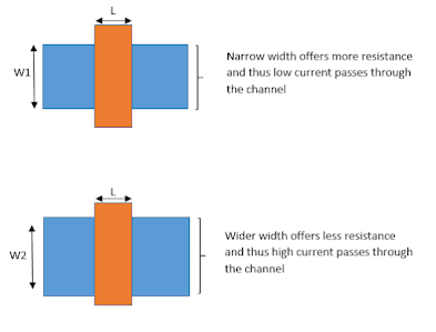
Case: I
ON Resistance is reduced with increasing the width of the channel as shown in the figure. W1 < W2, and L is same.
Width of the channel adds up to the height of the standard cell and if there is any restriction on the height of standard cell, we need to avoid changing width parameter of the cell/device(nmos or pmos).Instead we can the increase the width of the device indirectly by constructing more than one gates (fringes) and connecting them in parallel as show in below figure which increases effective width of the device.

Case II
By changing the channel also we can change the driving strength!!!……. But for technology node channel length is constant, then how can channel length be changed?
For a given technology node there will be more than one channel and this details are provided by fab people. I mentioned on channel length in my previous post Technology/Process Node
There raises a question when we need to upsize the drive strength?
When the load capacitance is more than the internal capacitance as a result charging time increases and delay increases, to reduce the charging time/delay we have to upsize the cell.
Clarification:
Lets us consider a CMOS design which has both nmos and pmos.The height of the cmos(standard cell) is equal to the sum of Vdd’s widht, pmos channel width, diffusion spacing between pull-up and pull-down transistors, nmos channel width and width of Vss metal layer. A clear picture was shown below. Thus changing the width of the channel in pmos or nmos effects the height of the standard cell

Where L represents the channel length of cell (pmos or nmos)
W represents the channel width of cell(pmos or nmos)


Thankyou for simple yet comprehensive explanation.
ReplyDelete